

Introduction
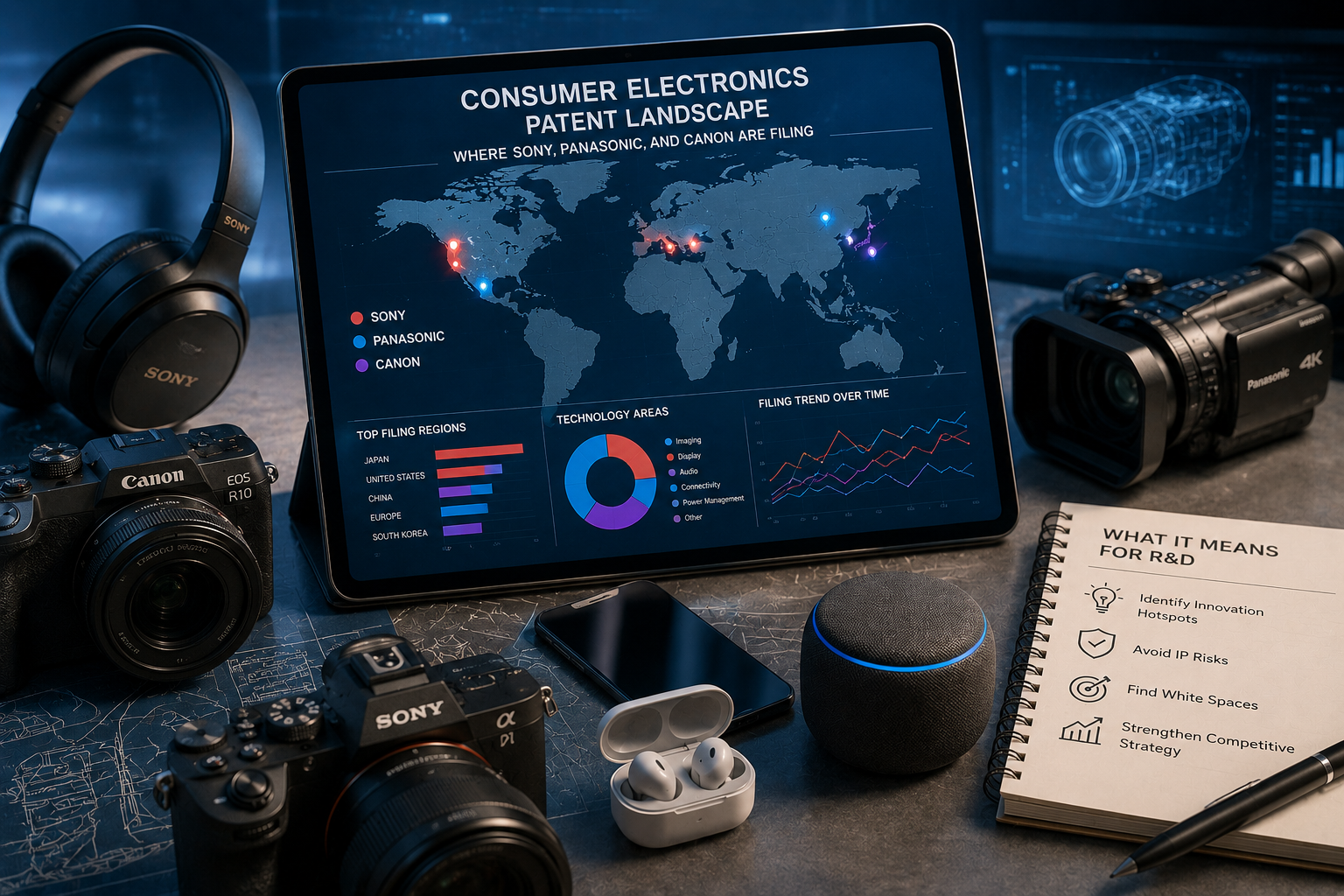
Three companies define the competitive IP picture in Japanese consumer electronics — but in three structurally different ways that create different landscape dynamics for R&D teams approaching their technology spaces. Sony’s portfolio is centred on image sensing, entertainment, and the semiconductor technology that underpins both. Panasonic’s portfolio has undergone a strategic transformation from consumer electronics to industrial and energy technology. Canon’s portfolio is among the deepest in precision optics globally, extending from camera systems into semiconductor lithography equipment that has little overlap with traditional consumer electronics but enormous commercial significance.
Reading these three portfolios accurately requires understanding not just what each company has filed but how each portfolio is structured, where the filing is concentrating, and — critically for R&D teams — where the intersections create cross-domain blocking risk for adjacent technology development. As our guide on the importance of patent landscape analysis to business strategy covers, the landscape is most actionable when it maps competitive IP at the level of specific sub-technology concentrations rather than at the level of top-line portfolio counts.
This article maps each of the three portfolios in turn, identifies what the filing patterns tell R&D teams about where the competitive IP is concentrating, and locates the whitespace that exists within and around each portfolio for teams with differentiated technology in adjacent spaces.
How to Read the Japanese Consumer Electronics Landscape
JPO classification structure for consumer electronics: Consumer electronics patents in Japan are classified primarily under JPO sections H (Electricity) and G (Physics), with the most relevant sub-sections covering image processing and display technology (G06T, G09G), audio and communication systems (H04N, H04R, H04S), optical systems (G02B), semiconductor devices (H01L), and battery and energy systems (H01M). Understanding these sub-sections is the starting point for scoping a Japanese consumer electronics landscape — because the same product category may have relevant patents distributed across multiple sub-sections that a broad classification search may not fully capture.
Why J-PlatPat is the essential starting point: J-PlatPat, the JPO’s official patent database, provides the most complete and current access to Japanese patent data including pending applications, granted patents, and prosecution history files. International patent databases have delayed and sometimes incomplete coverage of Japanese patent data relative to J-PlatPat. For a consumer electronics landscape focused on the Japanese patent landscape specifically, J-PlatPat search is the foundation layer — supplemented by international database searches for the same companies’ PCT and EPO filing activity.
How cross-licensing shapes the competitive picture: Japanese consumer electronics companies have historically engaged in extensive cross-licensing arrangements — particularly in display technology, audio systems, and optical components — that mean the blocking risk from any individual company’s patent portfolio is partially offset by existing licences among the major players. For R&D teams from outside this cross-licensing ecosystem entering Japanese consumer electronics technology spaces, the licensing landscape that mitigates risk between the incumbents does not automatically extend to new entrants. The competitive IP picture for a new entrant is therefore more exposed than it appears from the patent ownership data alone.
Sony’s Portfolio: Entertainment, Imaging, and Semiconductor Convergence
Image sensor technology as the dominant filing concentration: Sony is the world’s largest manufacturer of image sensors by revenue, and its patent portfolio reflects this market position. The CMOS image sensor sub-landscape — covering pixel architecture, readout circuit design, noise reduction algorithms, stacked sensor configurations, and multi-layer sensor integration — is among the densest in any single consumer electronics sub-technology. Sony’s image sensor patents are filed both at the JPO and internationally through PCT, and they cover not just sensor hardware but the image signal processing algorithms, HDR processing methods, and AI-assisted scene recognition systems that sit on top of the sensor hardware. For R&D teams developing products with integrated imaging capabilities, the Sony image sensor landscape is the most consequential FTO consideration in Japanese consumer electronics.
Entertainment and content delivery patents: Sony’s entertainment business — music, film, and streaming — has generated a significant patent portfolio around content delivery, digital rights management, streaming optimisation, and interactive entertainment systems. These patents sit at the intersection of consumer electronics and digital media technology. For companies developing streaming devices, content aggregation platforms, or interactive entertainment hardware, the Sony entertainment IP landscape represents a cross-domain blocking risk that a hardware-focused FTO search may not surface.
PlayStation and interactive entertainment IP: Sony’s PlayStation business has generated one of the deepest gaming hardware and software patent portfolios globally. Controller ergonomics and haptic feedback technology, GPU architecture for gaming applications, cloud gaming infrastructure, and social gaming platform systems are all areas where Sony holds active patent positions. For companies developing gaming peripherals, cloud gaming services, or interactive entertainment hardware, the PlayStation IP landscape is a distinct and commercially significant sub-landscape within the broader Sony portfolio.
Cross-Domain Risk: Sony’s image sensor leadership creates cross-domain risk in medical imaging, automotive cameras (ADAS), industrial machine vision, and drone-mounted cameras. R&D teams in these adjacent sectors frequently encounter Sony image sensor patents that were not anticipated in a search focused on the primary application sector. A medical imaging FTO that does not cover the Sony consumer image sensor landscape may miss blocking patents that read directly on the medical camera technology being developed.
Panasonic’s Portfolio: The Pivot from Consumer to Industrial and Energy
Battery and energy systems as the primary current filing direction: Panasonic’s strategic pivot away from consumer electronics toward industrial and energy technology is clearly reflected in its recent patent filing activity. Battery technology — particularly EV battery systems, battery management electronics, and energy storage system integration — has become the primary current filing concentration for Panasonic. This reflects Panasonic’s joint venture relationship with Tesla (Panasonic Energy) and its own EV battery manufacturing ambitions. For R&D teams in EV battery technology, Panasonic’s battery IP portfolio is a significant landscape consideration that sits in industrial and energy patent classifications rather than traditional consumer electronics ones.
Factory automation and B2B technology patents: Panasonic has built growing positions in factory automation, electronic component mounting systems, industrial laser technology, and B2B IoT systems. These filings reflect the company’s strategic repositioning as a B2B solutions provider rather than a consumer products company. For R&D teams in industrial automation or smart factory technology, Panasonic’s industrial technology portfolio is now a more relevant landscape consideration than its historical consumer electronics IP.
How Panasonic’s strategic pivot changed its landscape footprint: Panasonic has divested significant consumer electronics business units over the last decade — selling its TV business, restructuring its home appliance division, and exiting several consumer product categories. These divestments have been accompanied by corresponding changes in patent filing activity: declining filing rates in the divested consumer technology areas and increasing rates in energy, industrial, and B2B technology categories. For landscape analysis purposes, Panasonic’s patent portfolio is a transitional landscape — with legacy consumer electronics IP coexisting with an actively growing industrial and energy IP estate.
Canon’s Portfolio: The Depth of Precision Optics and Imaging
Optical design and lens system patents: Canon holds one of the deepest optical design patent portfolios globally. Lens design, optical element manufacturing, autofocus system architecture, image stabilisation mechanisms, and optical coating technology are all areas where Canon has decades of accumulated filing activity. For R&D teams developing optical systems — whether for cameras, medical endoscopes, industrial inspection systems, or automotive LiDAR — the Canon optics landscape is the most concentrated blocking IP in the relevant sub-classifications. The cross-domain risk from Canon’s camera optics patents into medical and industrial optical applications is particularly significant for teams that scope their FTO only to their primary application sector.
Printer and document management technology: Canon’s office technology business — printers, copiers, document management systems, and multifunction devices — has generated a dense secondary patent landscape in inkjet printing technology, laser printing mechanisms, toner formulation, and document workflow systems. For R&D teams developing printing or document technology, this sub-landscape is the most immediately relevant Canon IP consideration. It is also an area where Canon has been historically active in licensing and enforcement.
Semiconductor lithography equipment: a distinct and deep sub-landscape: Canon’s semiconductor lithography equipment business — producing the exposure systems used in chip fabrication — has generated one of the deepest specialised patent portfolios in any industrial equipment category. Photolithography optics, exposure system design, wafer alignment technology, and nano-imprint lithography systems are all areas where Canon holds significant active positions. This sub-landscape is entirely distinct from Canon’s consumer imaging business but represents the company’s most technically complex and commercially significant IP estate.
What the Three Portfolios Tell R&D Teams About Whitespace
Our guide on how patent landscape analysis can enhance your R&D strategy covers how landscape outputs translate into R&D investment decisions. For the Japanese consumer electronics landscape specifically, whitespace analysis reveals a consistent pattern: the densest blocking IP sits in the core technology areas of each company’s primary business, while the adjacent application sectors — where the companies’ technology is deployed in non-primary markets — are often less densely covered by their filing activity.
- Sony image sensor whitespace: While Sony’s core image sensor architecture and readout circuit patents are dense, the specific application layers for emerging sensor use cases — event cameras for robotics, time-of-flight sensors for AR/VR applications, and multi-spectral sensors for agricultural applications — have less concentrated filing from Sony specifically. For R&D teams in these emerging sensor application areas, the whitespace exists not in sensor hardware but in the application-specific signal processing and system integration patents around Sony’s hardware base.
- Panasonic transition whitespace: The gap between Panasonic’s historical consumer electronics IP and its current industrial and energy focus creates transitional whitespace in areas where neither the old nor the new filing strategy has concentrated. Smart home energy management systems, grid-edge storage control algorithms, and residential solar-battery integration technology are sub-categories where Panasonic’s filing is lighter relative to its commercial involvement.
- Canon optics whitespace: Canon’s optics patent depth creates the most accessible whitespace in the specific application integrations rather than the optical technology itself. Endoscopic AI-assisted diagnosis systems, LiDAR signal processing for automotive applications, and augmented reality optical waveguide integration are areas where the core optical technology may be blocked by Canon but the system integration and application intelligence layers offer genuine filing opportunities for R&D teams with differentiated capabilities in those integration layers.
How Our Landscape Analysis Service Covers Consumer Electronics
Our patent landscape analysis service covers the Japanese consumer electronics patent landscape with J-PlatPat-based search for each of the three major portfolio holders alongside the broader competitive field, filing trend analysis by sub-technology concentration, cross-domain risk identification for application-adjacent R&D teams, and whitespace analysis at the sub-classification level where differentiated technology can establish defensible IP positions. For R&D teams assessing entry into technology spaces adjacent to Sony’s imaging, Panasonic’s energy and industrial, or Canon’s precision optics portfolios, we provide a landscape analysis that maps the cross-domain blocking risk as well as the primary portfolio structure.
Mapping the Japanese consumer electronics patent landscape for R&D investment or market entry decisions? Our service covers Sony, Panasonic, and Canon filing patterns with cross-domain risk identification and whitespace analysis at the sub-classification level. → Contact Us
Conclusion: The Takeaway
The Japanese consumer electronics patent landscape is not one competitive IP picture. It is three distinct portfolio structures sitting in adjacent and occasionally overlapping technology spaces. Sony’s image sensor and entertainment convergence, Panasonic’s industrial and energy pivot, and Canon’s precision optics depth each create different competitive IP environments for R&D teams approaching their primary and adjacent technology spaces.
The landscape analysis that drives useful R&D decisions maps each portfolio at the sub-technology level — where the filing is concentrating, where the cross-domain risk for adjacent applications sits, and where the whitespace exists in the application integration layers that each company’s hardware-focused filing has left less densely covered. That level of precision is the difference between a landscape that confirms what R&D teams already suspect and one that reveals the specific filing opportunities they have not yet identified.