What is Extreme Ultraviolet Lithography (EUVL)?
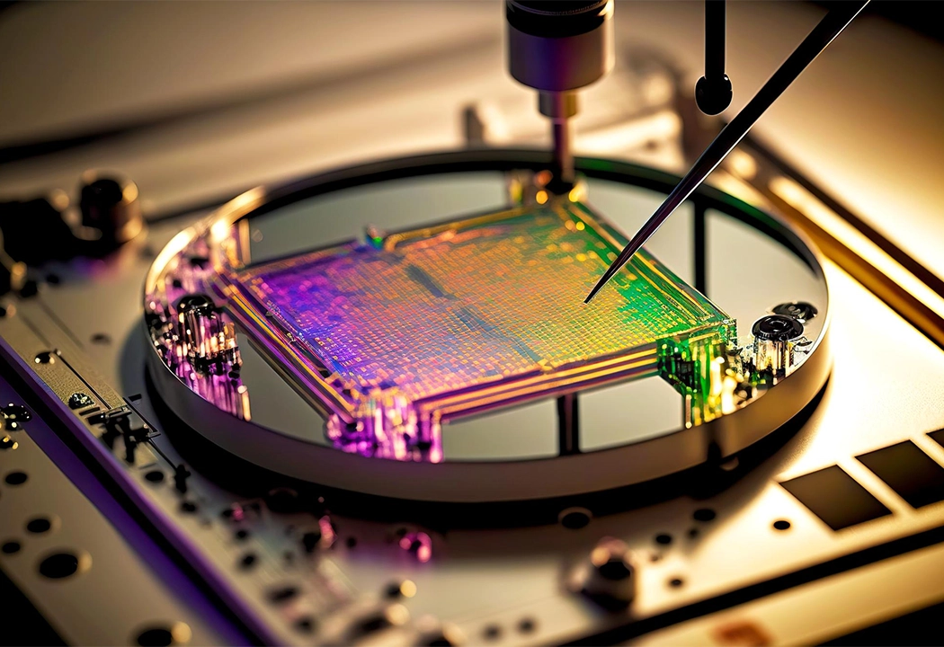
Extreme Ultraviolet Lithography (EUVL) represents a significant leap forward in semiconductor manufacturing, essential for the production of the next generation of microchips. This advanced technology, which operates at the cutting-edge of microfabrication, employs light at the extreme ultraviolet spectrum, typically around 13.5 nanometers, to etch incredibly small features on silicon wafers.
Confidently Tackle IP Research
Development and Challenges
The journey towards extreme ultraviolet (EUV) lithography has been marked by substantial challenges. Developing the technology required immense research, innovation, and investment.
The creation of extreme ultraviolet euv lithography light, for instance, is a complex process: it involves generating a plasma that emits the desired wavelength by firing high-energy lasers at molten tin droplets. The precision required in the production and maintenance of the equipment, like the mirrors and photomasks, is extraordinarily high.
Table of Contents
Industry Impact
The introduction of EUVL is a game-changer for the semiconductor industry. It has enabled the production of more advanced, efficient, and powerful microchips, crucial for modern electronic devices. EUVL’s ability to create finer circuitry on chips means that manufacturers can pack more transistors into the same space, significantly boosting performance and energy efficiency.
Adoption and Future Outlook
Despite its benefits, the adoption of EUVL has been gradual, primarily due to its complexity and high costs. However, industry giants such as Intel, Samsung, and TSMC have begun incorporating EUVL into their manufacturing processes.
This adoption marks a pivotal moment in the industry, showcasing a commitment to pushing the boundaries of what’s possible in semiconductor technology.
Broader Implications
EUVL is not just a milestone for the semiconductor industry; it’s a catalyst for broader technological innovation. Its implications extend across various sectors, including computing, telecommunications, and healthcare.
As EUVL technology continues to evolve and become more mainstream, it is expected to drive significant advancements in these and other fields.
Get Even More In-Depth Insight into the Extreme Ultraviolet Lithography (EUVL) Industry Through Our Report
Extreme Ultraviolet (EUV) Lithography Market Landscape
The Current Market Scenario
EUV Lithography has become a linchpin in semiconductor manufacturing, enabling the creation of ultra-small, high-performance chips. This technology is vital for a range of applications, from consumer electronics to high-end computing solutions.
Market Size and Growth
The EUV Lithography market has shown significant growth in recent years. As of 2023, the market was valued at approximately $9.4 billion, reflecting the burgeoning demand for advanced semiconductor technologies.
Looking ahead to 2028, market projections estimate a leap to around $25.3 billion, underscoring the technology’s critical role in the future of semiconductor fabrication.
Key Market Drivers
- Advancements in Computing Technology: The rise of AI, machine learning, and the need for high-performance computing have significantly driven demand.
- Miniaturization of Electronic Devices: The ongoing trend towards smaller, more efficient devices continues to push the boundaries of chip manufacturing.
- Innovative Breakthroughs in Semiconductor Manufacturing: EUV Lithography is vital as traditional lithography reaches its limits, making it a key technology for future developments.
Key Market Players
The market is shaped by a few key extreme ultraviolet lithography companies, each contributing significantly to extreme ultraviolet lithography market advancement
Market Challenges and Limitations
While promising, the EUV Lithography market faces several challenges:
- High Costs and Complexity: The sophisticated nature of EUV technology and its associated costs are major barriers to broader adoption.
- Technical Challenges: As chip features shrink further, yield, throughput, and complexity become more daunting challenges.
- Supply Chain Hurdles: The specialized nature of EUV equipment and high demand lead to significant supply chain challenges.
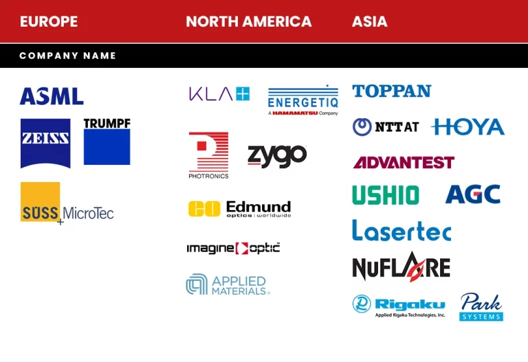
Regional Insights
This market has a global footprint with significant regional variances:
- North America and Europe: These regions are at the forefront, with major players like ASML and Intel.
- Asia-Pacific: Regions like Taiwan, South Korea, and China are rapidly emerging as semiconductor manufacturing hubs, with substantial investments in EUV technology.
The Future Outlook
The EUV Lithography market’s future is bright and filled with opportunity. The anticipated growth to $25.3 billion by 2028 speaks to the increasing demand and the technology’s expanding applications.
Innovations on the Horizon: We can expect future innovations to focus on improving efficiency, throughput, and cost-effectiveness. Integrating AI and machine learning into the manufacturing process could revolutionize EUV Lithography.
Impact on the Semiconductor Industry: EUV Lithography is set to redefine semiconductor manufacturing, enabling next-generation chips that will have wide-reaching implications across industries.
Extreme Ultraviolet (EUV) Lithography Patent Landscape
Patent Portfolio Overview
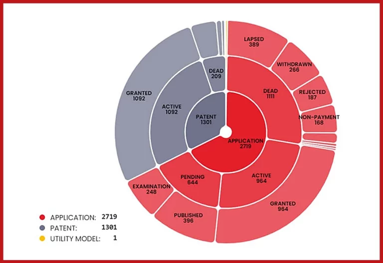
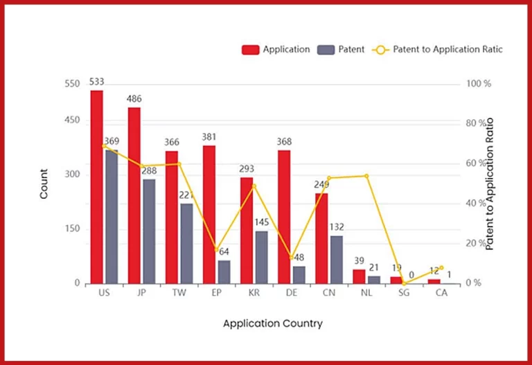
Country-wise Patenting Trends
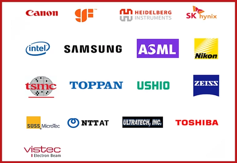
Major Players in EUV Lithography IP Landscape
Recent Advancements in EUV Lithography
High NA (Numerical Aperture) EUV Lithography
High NA (Numerical Aperture) EUV lithography is an evolution in chip fabrication, designed to address the limitations of existing EUV machines in achieving the fine resolutions required for sub-2nm nodes.
This advanced technique improves upon traditional EUV lithography by using larger optics to enable higher resolution patterns, crucial for the next generation of semiconductor manufacturing.
High NA EUV lithography focuses the EUV light more sharply, albeit with a shallower depth of focus, necessitating precision in the photoresist and mask designs to avoid any blurring. This method promises to be at the heart of future chip development, requiring deep industry collaboration for its successful implementation.
EUV lithography patterning using multi-trigger resist
The research into EUV photoresists, particularly with an eye towards high-NA EUV lithography, is progressing with the development of a multi-trigger resist (MTR). This new type of resist is designed to deal with the increased photon-shot noise expected in high-NA systems and aims for high EUV absorbance to maintain thin films despite the reduced depth of focus.
The MTR concept utilizes molecular materials to maximize resolution and minimize roughness, boasting absorbance greater than 18 μm-1. Recent experiments have shown promising results in patterning fine features with optimized dose requirements, showcasing the resist’s potential for future EUV lithography applications.
Carbon Nanotube EUV Pellicles
EUV pellicles are essential in the lithography process for protecting the photomask from contaminants. The quest for materials that can withstand the harsh conditions of high-power EUV scanners has led to the investigation of carbon nanotubes.
These materials are proving to be highly promising due to their robust mechanical and thermal properties, which are essential for enduring the extreme vacuum and venting environments within the scanner apparatus.
Their unique structure provides the necessary durability and the ability to endure high-energy exposure without degrading, ensuring the integrity of the photomask remains intact during the chip fabrication process. The continued development of carbon nanotube pellicles is expected to play a critical role in advancing EUV lithography technology.
Extreme Ultraviolet Lithography (EUV) Latest News
Intel’s Acquired High-NA EUV Scanner from ASML
Intel has recently received the first High-NA EUV lithography scanner from ASML, known as the Twinscan EXE:5000. This tool is designed to produce chips with process technologies beyond the 3nm scale, which the industry plans to adopt around 2025 – 2026.
The High-NA EUV technology, with its 0.55 numerical aperture lens, allows for 8nm resolution, improving upon the current 13nm resolution provided by existing EUV tools. This advancement means that chipmakers can avoid using double patterning in EUV, simplifying the manufacturing process while potentially improving yields and reducing costs.
Intel plans to start development work on its 18A node (1.8nm-class) in 2024 using these High-NA tools for future process nodes. This early adoption of High-NA tools could provide Intel with a competitive advantage in setting industry standards for High-NA manufacturing (Anandtech, 2024).
Furthermore, ASML has announced that it will be capable of producing 20 High-NA EUV lithography tools per year by 2027 – 2028, indicating that other industry partners are preparing to adopt these advanced systems in the coming years, with Intel leading the way by acquiring the majority of ASML’s machines in 2024 (Yahoo News, 2023).
$10B Earmarked for Development of Extreme-UV Lithography Center
In New York, Governor Kathy Hochul announced the creation of the High NA EUV Center at the Albany NanoTech Complex, a collaboration involving IBM and New York State, among other industry and academic partners.
This center will be North America’s first publicly owned R&D center with a High NA EUV system, which will be housed in a new building called NanoFab Reflection. The New York state and partners are investing $10 billion in this endeavor, aiming to drive semiconductor research and production in the US and create a large number of jobs.
The High NA EUV system at Albany NanoTech will be similar to future High NA EUV tools used in manufacturing facilities, ensuring that the processes and designs developed there will be transferrable to future electronic devices (IBM Research Blog, 2024).
In parallel, imec and Mitsui Chemicals have announced a strategic partnership to commercialize a key component for next-gen EUV lithography systems. They are focusing on EUV pellicles made from carbon nanotubes (CNTs), known for their strong mechanical and thermal properties.
The CNT-based pellicles boast more than 94% transmission of EUV light and can withstand EUV power levels beyond 1000 W. This development is crucial as the industry moves towards light sources exceeding 600 W to enable higher-quality nanoscale lithography (Optica-OPN, 2024).
Hitachi High-Tech Launches the GT2000
Hitachi High-Tech has launched the GT2000, a high-precision electron beam metrology system designed for the development and mass production of semiconductor devices in the High-NA EUV generation.
The GT2000 features new detection systems for advanced 3D semiconductor devices, a low-damage, high-speed multi-point measurement function for High-NA EUV resist wafers and aims to improve yield in mass production. It is specifically developed for the increasingly miniaturized and complex nature of advanced semiconductor devices.
SMEE Shanghai Micro Electronics Equipment Group Co. (SMEE), a Chinese company, has made a significant breakthrough in chipmaking technology. SMEE developed a lithography machine capable of manufacturing 28-nanometer chips.
This achievement is seen as a major step in China’s efforts to advance its semiconductor industry and reduce dependence on foreign technology, particularly in light of U.S. sanctions. The development indicates a significant reduction in the technological gap previously existing between Chinese and leading international semiconductor technologies.
DNP Develops Photomask Process for 3nm EUV Lithography
Dai Nippon Printing Co., Ltd. (DNP) has developed a new photomask manufacturing process for 3-nanometer EUV lithography. This advancement caters to the semiconductor market’s need for increasingly finer circuit line widths.
DNP’s history includes being the first merchant photomask manufacturer to introduce the multi-beam mask writing tool (MBMW) in 2016 and developing a photomask process for 5nm EUV lithography in 2020.
The new process leverages improved manufacturing techniques and data correction technology to support complex curved pattern structures, essential for EUV lithography. DNP plans to start operations with a new MBMW in the second half of 2024 and aims for annual sales of 10 billion yen in 2030.
Conclusion
Extreme Ultraviolet Lithography (EUVL) is a cutting-edge technology that has revolutionized how microchips are made. It uses very short wavelength light to create tiny and intricate patterns on silicon wafers, which are essential for making smaller, faster, and more powerful electronic devices like smartphones and computers.
Developing this technology was challenging and expensive, but it has had a big impact on the semiconductor industry. Companies like Intel, Samsung, and TSMC are using EUVL to make advanced microchips. Innovations such as High NA EUV lithography are making these chips even better by allowing even smaller and more detailed patterns.
The market for EUVL is growing rapidly, driven by the increasing demand for advanced electronics and the need for more powerful computing technologies.
About TTC
At TT Consultants, we're a premier provider of custom intellectual property (IP), technology intelligence, business research, and innovation support. Our approach blends AI and Large Language Model (LLM) tools with human expertise, delivering unmatched solutions.
Our team includes skilled IP experts, tech consultants, former USPTO examiners, European patent attorneys, and more. We cater to Fortune 500 companies, innovators, law firms, universities, and financial institutions.
Services:
- Patentability Search
- Invalidation Search
- Freedom to Operate (FTO) Analysis
- Patent Portfolio Management
- Patent Infringement Searches
- Drafting & Illustrations
- Competitive Benchmarking
- Technology Scouting
- Landscape Analysis
- Whitespace Analysis
- Business Research
Choose TT Consultants for tailored, top-quality solutions that redefine intellectual property management.
Contact Us