Introduction
Extreme Ultraviolet Lithography (EUVL) is an advanced technology using a light source of 13.5 nm and is a leading candidate for 22 nm node lithography and beyond. EUV lithography is now in the pilot phase with 0.33-NA tools at chip manufacturing sites. Mass-scale production is expected in near future.
EUV lithography tools use a plasma source to generate the 13.5 nm photons.
Patterns from a reflective mask are transferred to a substrate coated with light-sensitive material called photoresist. Patterning technique occurs in vacuum in all-reflective optics configuration. Fabricate integrated circuits with printed features smaller than 32 nm.
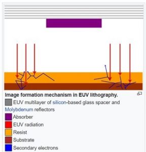
EUV light from plasma is collected into a collector that directs light into shaping optics called ‘illumination optics.’ The light illuminates a photomask. The illumination optics comprises multilayer-coated normal incidence mirrors and grazing incidence mirrors.
EUV masks are 6-inch square, 1/4-inch-thick low thermal expansion materials having multilayer reflective coating and an absorber layer etched into the circuit layer. The reflected image of the EUV mask enters the projection optic comprising six or more multilayer mirrors with NA > 0.25.
The final image is focused on a silicon wafer coated with a photo-sensitive etch resist or photoresist. The system operates in a low-hydrocarbon, high vacuum environment.
Among many challenges faced are light source, resists, and mask infrastructure and developing lithography tools which are economical.
Resist material must have high resolution, high sensitivity, low line-edge roughness (LER) and low outgassing simultaneously.
EUV – Technology Updates
- Multiple patterning
- Atomic Layer Deposition (ALD)
- Pellicle
- Dubbed High NA
- High-NA platform, called ‘EXE
EUV Lithography: What is next?
- The EUV lithography market is expected to grow from USD 2.98 billion in 2018 to USD 10.31 billion by 2023, at a CAGR of 28.16%.
- A major roadblock in EUVL – is a requirement of a high-power light source to illuminate the photoresist. ASML shipping equipment with 250W radiation power and the capability to generate 450W radiation.
- Another challenge in EUVL – is the strong absorption of EUV radiation by all materials. EUV resists are structured so that printing occurs in a very thin imaging layer at the surface of the resist. Further, EUV resists materials will have to evolve with the upcoming evolution in light source technology.
- Next-generation lithography beyond EUV includes X-ray lithography, electron beam lithography, focused ion beam lithography, and nanoimprint lithography. Nanoimprint is positioned to succeed in EUV due to its inherent simplicity and low cost of operation as well as its success in the LED, hard disk drive, and microfluidics sectors.